8 channel bridge input with a 24 bit sigma-delta ADC
8 full bridge channels
optimised for low power consumption (15 mW)
240 SPS max (all channels)
22 ENOB maximum at lowest sample rate, 16 ENOB at 240 SPS
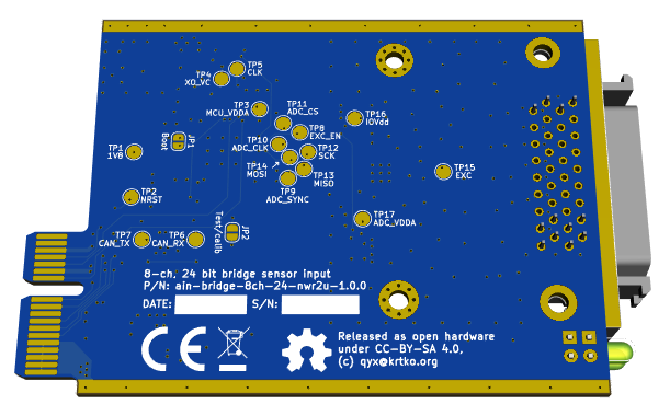
nwr-2u form factor (55 x 70 mm)
Warning
Documentation is WIP
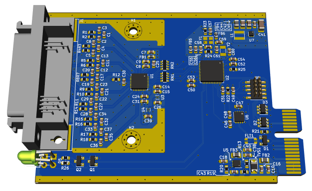
ain-bridge-8ch-24-nwr2u board is a 8 channel multiplexed digitiser for full bridge sensors, such as strain gauges. Sensors are excited with a 1.8 V voltage source and measured by a AD7124-8 analog-to-digital converter with a complete analog frontend comprising of a multiplexer, input buffers, programmable gain amplifier, sigma-delta modulator and configurable digital filters.
Conversion results are read by a microcontroller connected to the NW-R backplane using CAN bus.
Front panel includes a 36 pin MDR connector for sensors and two LEDs with configurable blinking pattern.
Project log
Date |
Description |
|---|---|
2021-05-29 |
1.0.0 prototype boards were submitted for manufacturing (JLCPCB) |
2021-06-22 |
Prototype boards have arrived |
2021-06-24 |
Two prototype boards populated |
2021-06-25 |
Testing firmware, ADC communication, configuration, conversion result reading |
Contents
Specifications
Operating conditions
Parameter (abbr.) |
Conditions |
Min |
Typ |
Max |
Unit |
|---|---|---|---|---|---|
Temperature |
-40 |
25 |
+85 |
°C |
|
Humidity |
non-condensing |
0 |
95 |
% RH |
|
Input voltage |
4.5 |
5.0 |
5.5 |
V |
Power consumption
The following figures are based on first measurements running testing firmware without all features enabled. The consumption may change a bit as a result of firmware optimisations and featureset changes.
Unless otherwise stated, measurements are done in the following conditions:
input voltage: 5 V
LED pattern: both LEDs disabled
no backplane communication
Parameter (abbr.) |
Conditions |
Min |
Typ |
Max |
Unit |
|---|---|---|---|---|---|
Input current |
continuous conversion of all 8 channels, 1 SPS |
2.0 |
mA |
||
. |
continuous conversion of all 8 channels, 30 SPS |
2.0 |
mA |
||
. |
continuous conversion of a single channel, 1 SPS |
2.0 |
mA |
||
Input current |
White LED fully on |
+0.6 |
mA |
||
. |
Blue LED fully on |
+0.6 |
mA |
Downloads (design files, firmware)
Description |
Download links |
|---|---|
Schematic (PDF export) |
|
Board layers (PDF export) |
|
Board manufacturing files (Gerbers) |
|
KiCad project files |
Notes
The board was designed and drawn in about 15 hours. Many compromises have to be made in order to finish the board withing the specified time. Hence, some wanted features were not implemented. When the board is validated in the field and gives reasonable measurement results, these features will be implemented in next revisions:
programmable excitation voltage from about 1 V to 10 V, probably using a SMPS buck-boost with a linear post regulator